How To Find Defects On A PCB?
PCBs are the backbone of electronic circuits, so it is very important to ensure that they are mechanically operational at all times. PCBs also guarantee proper connections between components and different parts of the circuit, which is essential in various functions such as sending and receiving data, calculating electrical parameters, amplifying electronic signals, etc.
PCB manufacturers guarantee optimal quality during mass production of boards. However, there are times when the PCB may be bad or defective due to a number of reasons. These defects lead to various problems and complications regarding the operation of the electronic circuit, since they compromise the performance of various components present in the circuit.
There are several types of problems or defects that can have an adverse impact on the desired performance of a circuit. Some of them are:
Defects caused during manufacturing and storage
Similar to other electrical components, PCBs are sensitive to different environmental factors such as temperature, humidity, contaminants, etc. During manufacturing and storage, various defects are observed in PCBs, some of which are:
Temperature : In the course of storage, as well as during component installation, PCBs are affected by temperature. In extreme conditions, various fluctuations in temperature occur that can be a potential factor that causes failures in components or joints.
It is essential to consider the maximum or minimum operating temperatures of PCBs during the design phase. Expansion and contraction of PCBs due to temperature fluctuation can ultimately cause PCB failure.
Moisture: During PCB manufacturing and storage, exposure to moisture can cause short circuits and could lead to defects in various circuit components. Moisture is present in the air and can damage the weld, which in turn causes corrosion.
Contaminants : Contaminants create defects during manufacturing and where PCBs are stored after the manufacturing process. If PCBs are exposed to factors like dust, insects, pollution, etc., they eventually end up weakening their performance.
Impact: Impact on PCBs can have a catastrophic effect during board manufacturing, storage, and transportation. If PCBs are dropped roughly or not manufactured correctly, they cause excessive vibration. Because of this, PCBs lose their flexibility, which in turn damages the traces on the boards.
Weld defects
Pushback of PCB traces due to a wrong solder joint causes a solder defect and can be minimized during the design and welding process.
Some of the most common weld defects are:
Open Joints: Also called natural solder, dry joints, or dry joints, open joints occur when the solder does not have a point of contact with the PCB pad. Open joints are mainly caused by physical movement or bending, incorrect soldering temperature, or vibrations of the PCB during shipping.
Excess solder: During the soldering process, sometimes due to late removal of the solder, there is an excessive build-up of induced solder on the components. This increases the risk of solder bridging and could play havoc with circuit connections.
Component displacement : This happens when the components placed on the PCB do not line up correctly during soldering. Component displacement can lead to open junctions and crossed signal lines that can cause disparities in the electronic circuit. There are several reasons why component shifting can occur, including heat sinks, solder temperature variations, manufacturing error, design error, etc.
Entanglement and Spatter: It is known as entanglement and spatter when different contaminants in the atmosphere affect the soldering of a PCB. Such defects lead to short circuit hazards, and they can also lead to change in the visual appearance of the PCB.
Raised Pads : Pads that become disconnected or separated from the PCB surface are called raised pads. This causes irregularities in the connection of the circuits, which, in turn, results in a malfunction of the printed circuit board. This problem is commonly found on single-sided PCBs, which contain a thin layer of copper with no through-hole plating.
Solder Balls: Occurs due to poor conditions such as gassing of the flux or excessive turbulence when the solder flows backwards. Considering the no-clean process, the numerous solder balls on the PCB can form a false bridge between two adjacent traces, causing circuit breakdown.
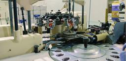
Machinery Defects: CNC milling machines are used to route, cut, and profile the board during the PCB manufacturing process. CNC machine robot unloading and board holes out of tolerance range in horizontal and vertical direction sharpen board unloading knives. This causes a collision that leads to edge collapse on a printed circuit board.
During extremely high volume production, CNC machines are subject to overheating. Therefore, it must be ensured that the machines are not operated in excess of 150 degrees Celsius, as this can lead to deterioration of the quality of the plate, wrong alignments, incorrect edging, etc.
Defects caused by electrostatic discharge
PCB damage from electrostatic discharge is very difficult to detect. Electrostatic discharge causes multiple short circuits that soften the weld. Both humans and machines can be the cause and must be carefully detected during the manufacturing and assembly process. Electrostatic discharge is one of the main reasons for PCB failure and can make components less resistant to short bursts of high voltage.
It is very important to locate and identify defects on the PCB during production. Defects in the PCB, if not detected in advance, can have drastic and dangerous repercussions in the future, both for the circuit and for the user who uses it.


